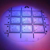
The backbone of the cleanroom is the lithography capability, the techniques by which design patterns are transferred to a sensitive resist as the initial stage of a fabrication process. In the Centre, the lithography is a mixture of electron beam lithography (>6 nm), 200 mm DUV KrF laser scanner lithography (>200 nm) and more traditional UV contact lithography (>800 nm). The Centre also has alternative nanopatterning techniques available such as Nano Imprint Lithography.
The mask aligners operate in contact or proximity modes and can handle a wide range of substrate sizes from small pieces up to 200 mm wafers. The Centre also has an extensive and versatile facility for resist processing, including a spray coater/developer for non-planar surfaces and the normal range of equipment such as spinners. The types of resist that are standard in the Centre is similarly extensive, from photoresists, ebeam resists through to thick film resists such as SU-8 and laminatable epoxy and acrylic materials.
EVG 620 TB - double sided mask aligners
This is a high precision, automated mask aligner capable of aligning both top and bottom side patterns on wafer sizes up to 200 mm. It is also paired with the EVG 520 bonder to provide the ability to precision align wafer stacks prior to bonding on substrates up to 150 mm.
Nikon KrF laser NSR-S204B scanner
Scanner for deep ultraviolet (DUV) lithography for patterning 200 mm diameter wafers. The scanner allows patterning of features with the critical dimensions down to 200 nm on 200 mm (8") diameter semiconductor wafers. Light source is provided by a KrF laser emitting at 248nm.