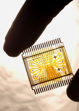
Associated with the Centre's interests in MEMs, microfluidics and packaging technology, there is a facility for wafer to wafer precision aligning and bonding. The alignment functions is provided by specially designed tools for the double sided aligner, which are then transferred to the bonder. We have the capability for thermal compression bonding, anodic bonding, fusion bonding and UV exposure bonding on wafer sizes up to 150mm. For R&D purposes, the machines are also capable of operating on pieces down to 15mm in size.
EVG 620 TB - double sided mask aligner
This is a high precision, automated aligner capable of aligning wafers (up to 150mm) on both top and bottom side features. Automated top and bottom alignment using specially designed marks is also possible.
EVG 520 TB - bonder
This a thermal bonder, capable of producing contact forces up to 20 kN and temperatures in excess of 400°C, with an excellent degree of uniformity and stability across wafer sizes up to 150 mm.
- Direct bonding
- Anodic bonding
- Eutectic bonding
- Adhesive bonding
- Hot Embossing
- Nano-Imprint Lithography
Direct bonding:
Direct or fusion bonding is a process that uses no intermediary layers and relies on intermolecular interactions such as van der Waals forces, hydrogen bonds and strong covalent bonds. Post-bond annealing is often used to maximize the bonding strength.
Applications:
Silicon on insulator (SOI) wafers
Sensors
Actuators
Capability:
100 mm (4”) and 150 mm (6”) wafers
Si to SiO2
SiO2 to SiO2
Al2O3 to SiO2
Process parameters:
Force 0 to 20 kN
Temperature RT to 500°C
Vacuum <= 1e-5 mbar
Pre-bond alignment
Post-bond annealing
Anodic bonding:
Field assisted bonding of Si or metal to glass. Commonly used glasses are sodium containing substrates such as Borofloat or Pyrex. These glasses have a similar coefficient of thermal expansion (CTE) to Si in the applied temperature range, which reduces the stress at the bonding interface. Bonding is done below the glass transition temperature (Tg) and with applied voltages in the kV range.
Applications:
Microfluidics
Process parameters:
Temperature ~400°C
Voltage ~1000 V (~1700 V for triple stack bonding)
Force ~1 kN
Eutectic bonding:
Eutectic bonding uses an intermediate metal layer such as Au or Al to facilitate bonding. Au or Al is chosen because of their ability to alloy with Si. Si-Au eutectic bonding is commonly used because of its relatively low eutectic temperature (~370°C), widespread use in die bonding and compatibility with Al interconnects.
Adhesive bonding:
Adhesive bonding uses an intermediate layer often an epoxy based, photosensitive resist to facilitate bonding. It can be patterned and used in non-hermetic applications and has strong adhesion to silicon and glass. Maximum bond strength is achieved with a post bond hard bake.
Applications:
Microfluidics
Encapsulation
Low temperature processing
Process parameters:
Force ~ 10kN
Temperature polymer dependant
Hot Embossing:
Hot embossing utilises pattern transfer from a master stamp/mold into a polymer. The inverse pattern from the stamp is transferred to the polymer. Polymers often used are PMMA, COC, etc. The embossing process involves applying force to the stamp while heating the polymer above the glass transition temperature (Tg). The master stamp/mold is generally formed in Ni and creates a robust and reusable way to replicate features.
Applications:
Microfluidics
Biosensors
Microneedles
Process Parameters:
Temperature <150°C
Force ~ 3-5 kN
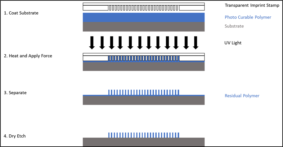
Nanoimprint Lithography (NIL):
Nanoimprint lithography is a fabrication technique used for low cost, high throughput, and high-resolution nanometre scale patterns. There are 3 main subcategories with NIL:
Thermoplastic nanoimprint lithography (T-NIL): Spin coating thin layer of thermoplastic polymer on to substrate, transfer mold pattern into polymer film, dry etching to transfer pattern to substrate.
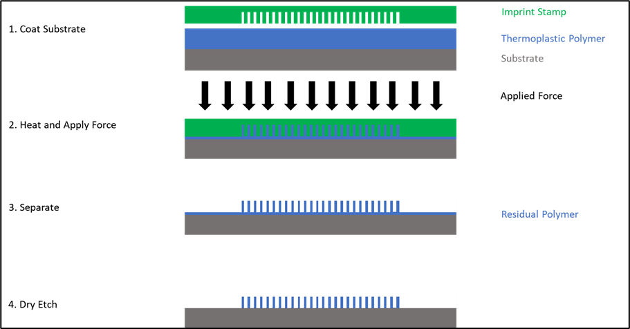
Photo nanoimprint lithography (P-NIL): Spin coating with photo curable liquid resist, transparent stamp, UV Cure, separation
Resist-free direct thermal nanoimprint lithography (Hot Embossing): Force and temperature to directly transfer stamp into a thermoplastic polymer.