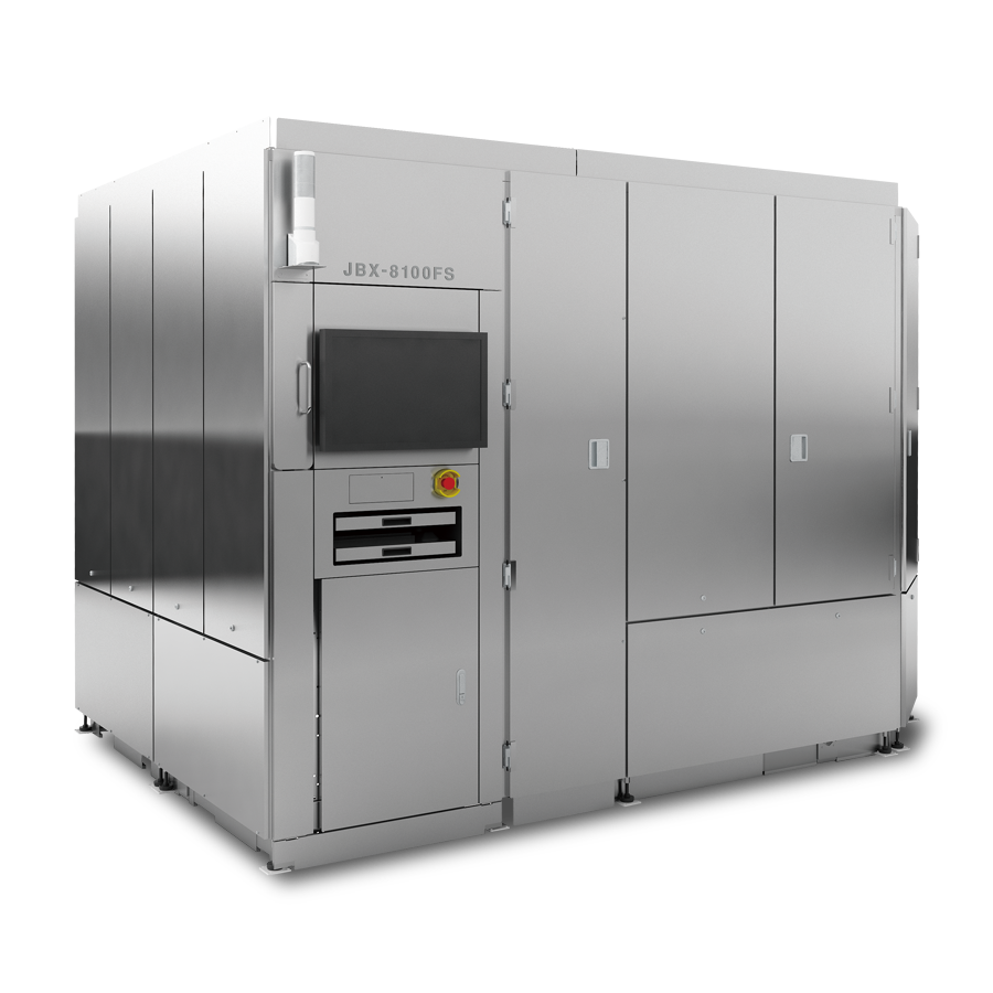
The Southampton Nanofabrication Centre (SNC) is the first academic institute in the world outside of Japan to host a JEOL 200 keV electron beam lithography system from the JBX-8100 G3 range. This state-of-the-art equipment is also equipped with a 200MHz scanner and has a minimum spot size of 1.8 nm, which enables sub 10 nm resolution (6 nm achieved). The field stitch and overlay accuracy is approximately 10 nm. The system has the ability to process a wide range of substrates, including transparent substrates, without the need to pre-coat before exposures. The substrate size can also vary from 3 mm chips up to 200 mm (8”) wafers. The tool is equipped with an autoloader that enables intake of multiple wafers at a time.
Patterns can be rapidly created from CAD files, without the need for a photomask, allowing quick turn around on design modifications. We hold licence for Genisys: BEAMER software for pattern optimization to enhance the high-resolution and throughput of the e-beam.
The system is an ideal fabrication tool for basic to advanced nanoscale research activity. It is capable of patterning a writing field area of 0.5 mm x 0.5 mm in high resolution mode (1 mm x 1 mm at 100 keV) and has a maximum wafer size of 200 mm in diameter.
Specifications
- JBX-8100 G3 e-beam writing system
- 1.6nm diameter Gaussian spot electron beam
- 100kV and 200kV accelerating voltage
- 50pA – 200nA current range
- 200MHz scan speed
- +/- 100µm vertical range automatic focus
- Vector scan for beam deflection
- Max 200mm (8") wafers with 7" of writing area
- < 10nm line width (6 nm produced)
- < ±10nm field stitching accuracy
- < ±10nm overlay accuracy
Sub- Category: Resist Processing
Our Nanofabrication facility has an extensive and versatile facility for resist processing such as spinners and developers for a range of materials like negative, positive, lift-off resists, coating and polymers for e-beam and optical lithography. We have hot-plates and ovens for post/pre-bake motive that can contain substrate sizes up to 200mm. We also have a mask cleaning or lift-off system for heated, high-pressure or spray dispensing of developer, lift-off solutions and DI water that can handle wafers up to 200mm and 230mm masks.