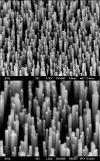
Nanowires and nanotubes are generally grown by bottom-up self-assembly. The nanowire and nanotube growth is catalysed using metallic or semiconducting nanoparticles and a chemical vapour deposition process is used to grow the nanowires or tubes from the vapour phase. Melting of the nanoparticles occurs prior to growth and for this reason the process is known as Vapour-Liquid-Solid (VLS) growth. The diameter of the nanowire or tube is determined by the size of the catalyst nanoparticle. The nanoparticles can be produced by evaporating or sputtering a thin metal layer and then annealing.
OPT Nanofab 1000 agile
This system is used to deposit carbon nanotubes and silicon, silicon-germanium and germanium nanowires. Catalyst nanoparticles are needed to initiate nanotube or wire growth, which usually takes the form of metal nanoparticles generated on the surface of the wafer prior to deposition. If the nanoparticles are omitted, the system can be used to produce silicon, silicon-germanium, germanium and SiC films. The nanowires can be doped either n-type (phosphorus) or p-type (boron) during deposition (i.e. in-situ doping). A deposition temperature up to 1000C can be used, allowing the silicon to be deposited as polycrystalline (~600C and above) or amorphous (<540C) material. For silicon-germanium slightly lower temperatures can be used and for germanium slightly lower still. The system can accept wafers up to 200mm in diameter and can do depositions on small pieces of silicon placed on a larger wafer. This is recommended to minimize cost when doing lots of trial depositions to set up a new process.

