PECVD is a technique for depositing a variety of materials that are commonly used in the semiconductor industry. The reactants are gases and energy is provided partly by heating the substrate to a high temperature (typically 400C or below) and partly by the plasma. Since the reactants are gases, deposition can be performed in principle on any substrate. The use of a plasma allows deposition to be done at a lower temperature than is possible with alternative techniques, such as low pressure chemical vapour deposition (LPCVD). However, the lower deposition temperature may lead to poorer material properties (e.g. lower breakdown voltage in the case of insulators). Material properties can often be improved by annealing at a higher temperature, which is referred to as densification.
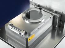
OPT Plasmalab System 100 PECVD: amorphous silicon deposition
This system is used to deposit amorphous and polycrystalline silicon, germanium and silicon-germanium. The material can be doped either n-type (phosphorus) or p-type (boron) during deposition (i.e. in-situ doping). A deposition temperature up to 650C can be used, allowing the silicon to be deposited as polycrystalline (~600C and above) or amorphous (<540C) material. For silicon-germanium slightly lower temperatures can be used and for germanium slightly lower still. The deposition rate for amorphous silicon is >25nm/min and for polysilicon is >40nm/min. The system can accept wafers up to 200mm in diameter and can do depositions on small pieces of silicon placed on a larger wafer. This is recommended to minimize cost when doing lots of trial depositions to set up a new process.
OPT Plasmalab System 100 liquid source PECVD: nitride & oxide deposition
This system is used to deposit silicon dioxide, silicon nitride and rare earth doped oxides. The machine has two liquid precursors, one for TEOS and one for rare earth doped oxides. For high vapour pressure liquid sources, argon is bubbled through the liquid precursor to provide a vapour for the PECVD, whereas for low vapour pressure liquid sources the bottle is just open to the deposition chamber. TEOS is used to deposit silicon dioxide at 350-400C and has good planarising properties for metallization. The system has a low frequency and high frequency (RF) plasma source and the two sources can be combined to deposit layers with low stress. For TEOS the deposition rate is >40nm/min. Silicon dioxide can also be deposited using SiH4/N2O/N2 at 300C with a deposition rate of >40nm/min. Silicon nitride is deposited using SiH4/NH3/N2 at 300C with a deposition rate of >10nm/.min. The system can accept wafers up to 200mm in diameter and can do depositions on small pieces of silicon placed on a larger wafer. This is recommended to minimize cost when doing lots of trial depositions to set up a new process.
OPT Nanofab 1000 agile : nanotube & wire deposition
This system is used to deposit carbon nanotubes and silicon, silicon-germanium and germanium nanowires. Catalyst nanoparticles are needed to initiate nanotube or wire growth, which usually takes the form of metal nanoparticles generated on the surface of the wafer prior to deposition. If the nanoparticles are omitted, the system can be used to produce silicon, silicon-germanium, germanium and SiC films. The nanowires can be doped either n-type (phosphorus) or p-type (boron) during deposition (i.e. in-situ doping). A deposition temperature up to 1000C can be used, allowing the silicon to be deposited as polycrystalline (~600C and above) or amorphous (<540C) material. For silicon-germanium slightly lower temperatures can be used and for germanium slightly lower still. The system can accept wafers up to 200mm in diameter and can do depositions on small pieces of silicon placed on a larger wafer. This is recommended to minimize cost when doing lots of trial depositions to set up a new process.
OPT FlexAl RPX: Atomic Layer Deposition
This system is equipped with four liquid precursor modules and hence can deposit up to four different ALD layers in the same run. It can be used to deposit HfO2, TiN, ZnO and Al2O3 using TEMAH, TiCl4, DEZ and TMA precursors respectively. The deposition rate is typically between 0.2 and 1.5 angstrom per cycle. The system can accept wafers up to 200mm in diameter and can do depositions on small pieces of silicon placed on a larger wafer. This is recommended to minimize cost when doing lots of trial depositions to set up a new process.